
In the first exciting part of this series we got to the point of a completed design for the CPU board. By this point I’d got a PCB and working system. I realise that I have skipped two topics that need to addressed now. The keypad/display, and an interim solution to the INS8514 I/O device.
First we need to talk about the INS8514. Initially I wanted to change the original design as little as possible so wanted to support this I/O chip natively whilst I proved my design worked, but ultimately I wanted to move away from this device. I do have a couple of these ICs so I managed to use one to debug my system and get it working. After a bit of reading and research I found that I could probably use the 6522 VIA with just a few pinout modifications; and the loss of the 128 bytes of RAM. I wasn’t concerned about the loss of RAM as nothing really uses it and today RAM is cheap so it’s much more economical to add a large RAM expansion board to the system if needed.
After some experimentation I came up with this.
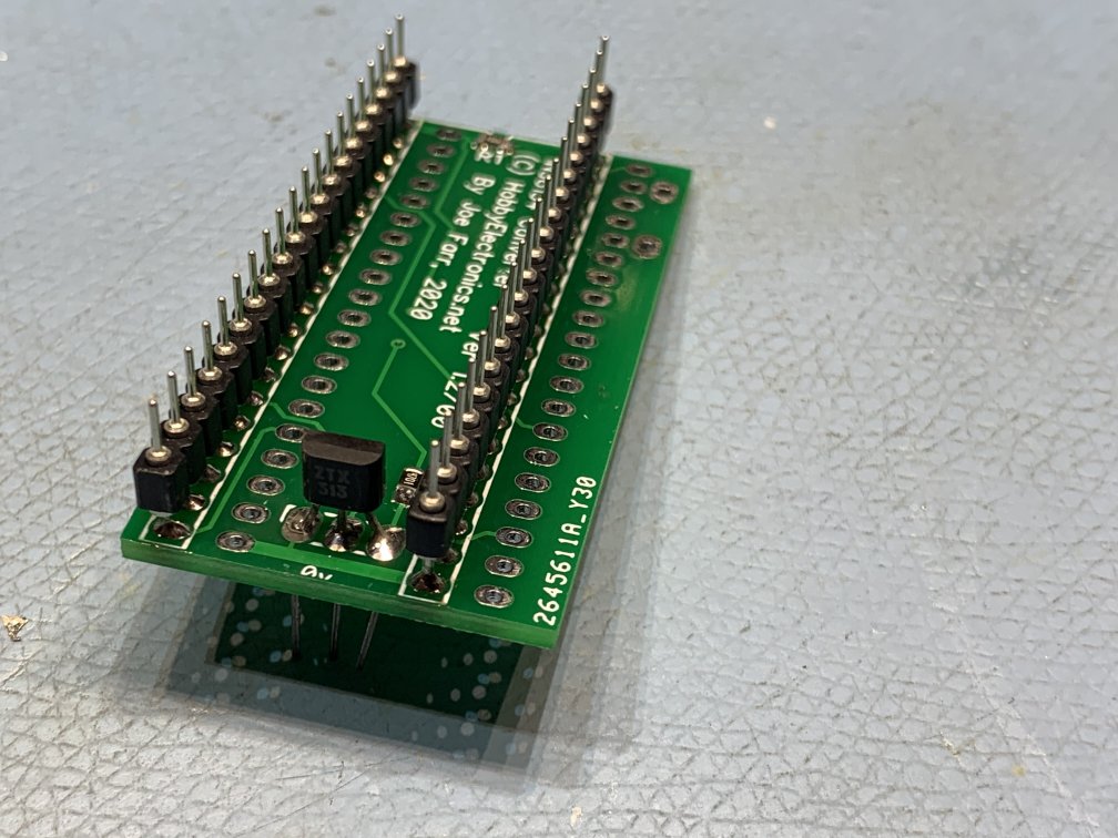
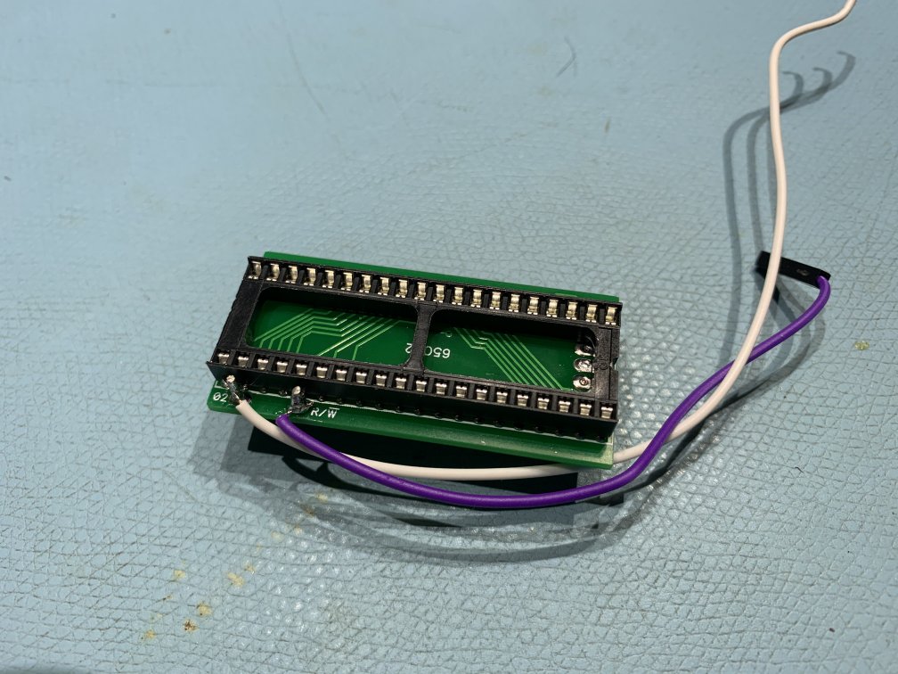
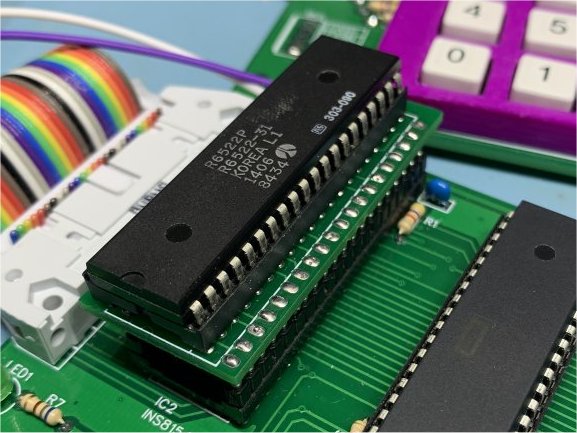
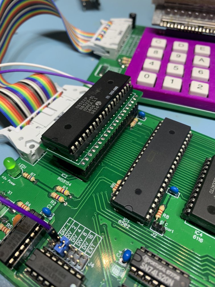
It’s a small piggyback board that plugs into the original INS8514 socket allowing a common 6522 VIA to work. It needs a couple of external signals to work correctly but other than that it just plugs in. More importantly no software changes to the Monitor firmware are required. The PCB files are available and could be useful for uses of an original system if they cannot obtain an INS8514. Later CPU designs would move away from the INS8514 completely and natively adopt the W65C22, which is faster than the standard 6522.
Next, the key pad & display board. This is basically the same as the original with one major exception in that it no longer has the cassette interface electronics. I decided that I would not be saving and loading data via the cassette interface so didn’t want to have the hassle of adding that to the board. However, I did leave a small connector that can could be used to connect to a separate cassette interface board if required.
The final version of the keypad/display board does support the original bubble LED displays but I found that the replacement 6522 VIA can’t drive the display as brightly as the original INS8514 and it was rather dim in use. So I made provision to be able to add a different display if required. Compatibility is maintained with the original displays if required.
I used different PCB switches than the original so my keypad is slightly larger.
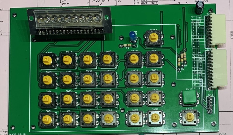
The above image is of the first version of the replica display/keypad PCB. There were a couple of improvements over the original; a power LED for one thing, and the NMI and IRQ buttons that were on originally on the CPU board have been relocated here.
Unfortunately not all my brilliant ideas were… well, brilliant. You can see on the right-hand side I decided to add connectors for the ribbon cable that links the PCB to the CPU board (unlike the original that used a soldered ribbon cable). I elected to use Molex connectors as that’s what I had, which turned out to be a stupid idea. They were so stiff that when pulling on the cable to remove them the pins would pull out of the shells. This was also when I discovered that the original bubble LED displays were rather dim, so I made provision on the display connector to support a powered display.
These and several other updates lead to the final version shown below.

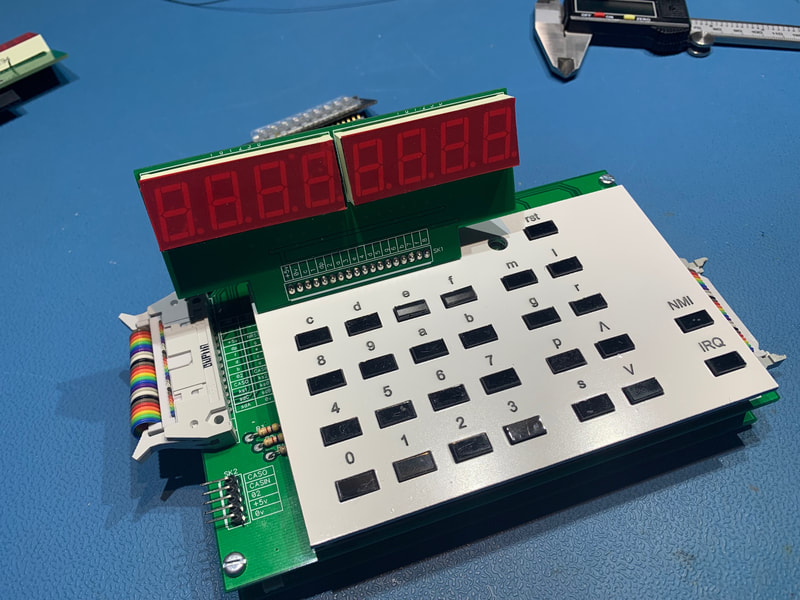
I’ve now made some custom keycaps to better replicate the original and the board can be used with the original bubble LED display, or the new brighter and larger LED display.
There is a post here with more information about the keypad and how I created the fascia and keycaps.
So at this point my System 1 runs. I was writing small test programs utilising the internal 2K of RAM and doing things on the display without any problems, all whilst running the CPU at a blistering 8MHz. However, what this system needs is I/O devices… so that’s the next job.
Construction details, schematics and plans can be found here.
Leave a Reply
You must be logged in to post a comment.