
As a recap, I’ve got a runnable system. Programs can be entered into the systems memory in hex using the keypad and display then executed. However, as it stands there are no additional input or output devices; only the keypad and the LED display and it’s all a bit limiting really.
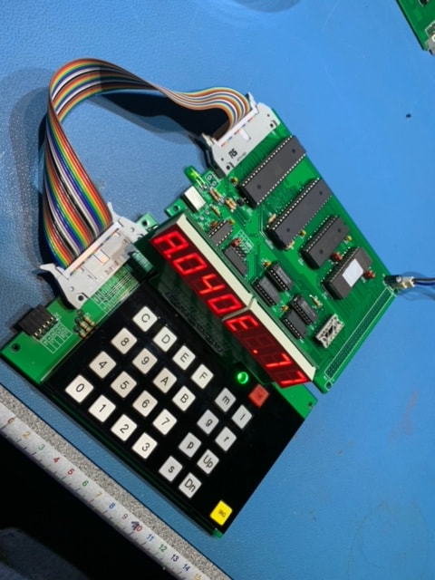
It’s possible to separate the CPU and Keypad/display boards (as shown in the above image), add an edgeway connector to the CPU board and insert it into a backplane. From here it’s then possible to add additional I/O cards to the backplane and grow the system into a fully functioning general purpose computer.
Step 1, design a backplane.
I decided to design a small 3-slot backplane with onboard 5v regulated PSU to drive everything. Later on I would design a larger backplane.
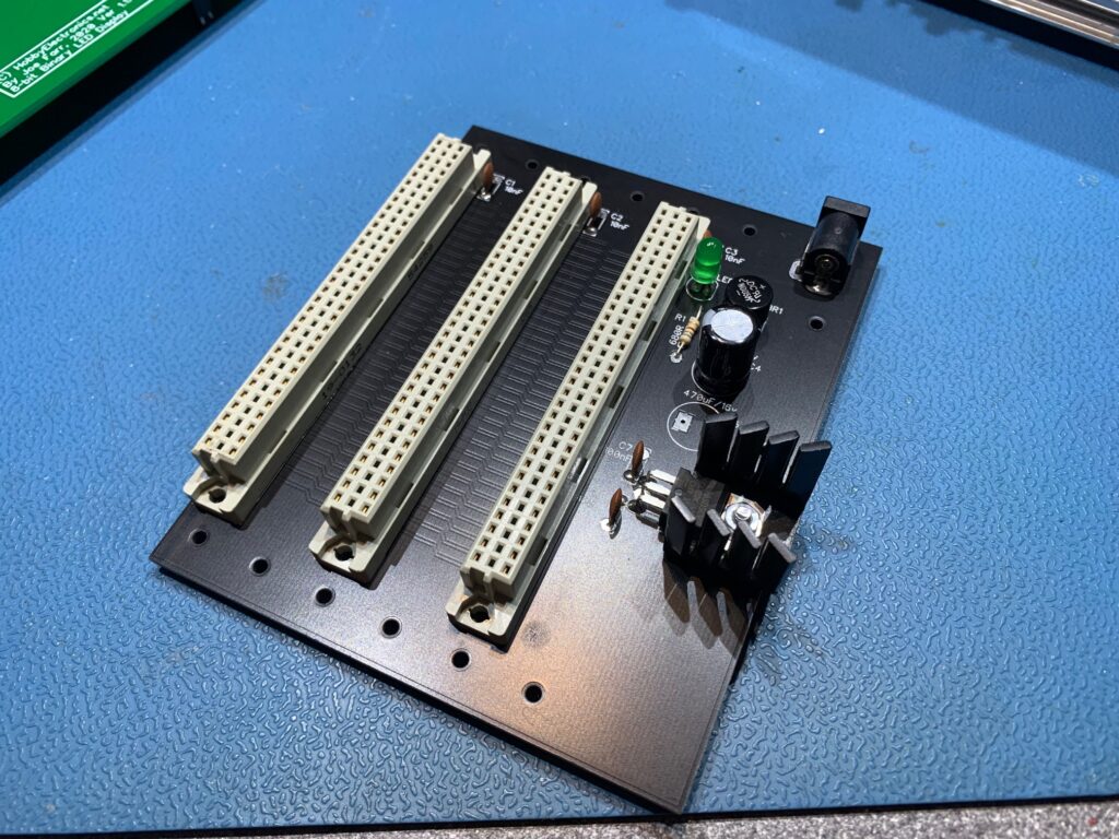
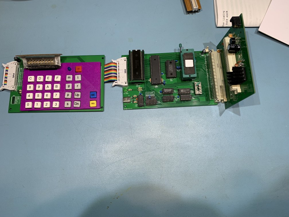
The above shows the simple 3-slot backplane and the CPU card plugged in.
Now at this point I’m going to take an alternative path than expected with the hardware. The System 1 CPU, Keypad and 3-slot backplane are great as they are and should be pretty much compatible with real System 1 hardware.
However, I wanted to do things differently and from this point on, compatibility with the Acorn universe will be broken.
Address Decoding
If you’ve worked with expandable microprocessor systems before, one requirement for each expansion card is to be able to decode an address, or range of addresses so the CPU can talk to, or address that specific expansion card. It get’s a bit complicated and I’m not going to go into any real detail here, but our 6502 CPU supports a 64K (Address $0000 to $FFFF) or 16-bit address range. You pick an address or range of addresses for your hardware expansion card to live in, set the expansion card to respond to that address(s) and away you go. The problem is some addresses are simpler to specify than others. If your address range falls on a nice convenient boundary; i.e. $1000 to $1FFF then it’s pretty simple and doesn’t require much in the way of address decoding. However, if you want to use a single address or small range of addresses i.e. $1000 to $1005 it starts getting more complicated and more electronics are required, and it occurred to me that if you want the ability to place expansion cards anywhere in the memory map, the address decoding could get rather complex and would need to be included on each expansion card. This seemed such a waste.
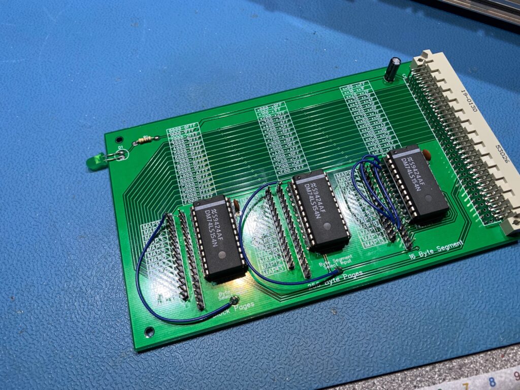
Enter the SAD – Segment Address Decoder
When designing the PCB I realised that not all of the 64 connections on the PCB expansion connector were used so decided to reserve 14 of them for SAD addresses. The SAD card is programmed with ranges of addresses you want to decode, and when an address falls within a specified range, the appropriate SAD address signal is asserted. A SAD address can be a single address or a block of addresses. If you are smart in the way memory addresses are utilised you can decode addresses for an entire system using just one SAD expansion card. You can however install as many SAD cards as required. This saves a lot of additional electronics on each expansion card.
Simply put, a single SAD expansion board can decode one or more 4K address blocks, one or more 256 byte pages or one or more 16 byte segments.
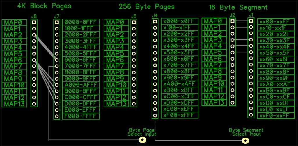
The above diagram shows how the SAD works. There are 14 SAD address range outputs labelled MAP0 to MAP13. These 14 signals are presented to all expansion slots so accessible by all expansion cards. Each card uses as many MAP signals as required.
As many 4K address blocks as required can be allocated to 1 or more MAP signals. In the above diagram, addresses $6000-$6FFF (4K) are assigned to MAP2 and address range $A000 to $DFFF (16K) are assigned to MAP6
Address range $7000 to $7FFF is then fed into the next level of address decoding. One or more 256 pages can be decoded from the $7000 to $7FFF range. These 256 byte page addresses can themselves be connected to MAP signals. One of these 256 byte pages can then be further decoded to 16 byte segments. In the example above, $xx00 to $xx0F are assigned to MAP0, $xx10 to $xx1F are assigned to MAP1 and so on. This one expansion card is therefor providing multiple address decode signals for multiple expansion cards thus reducing the amount of decode logic required in the system.
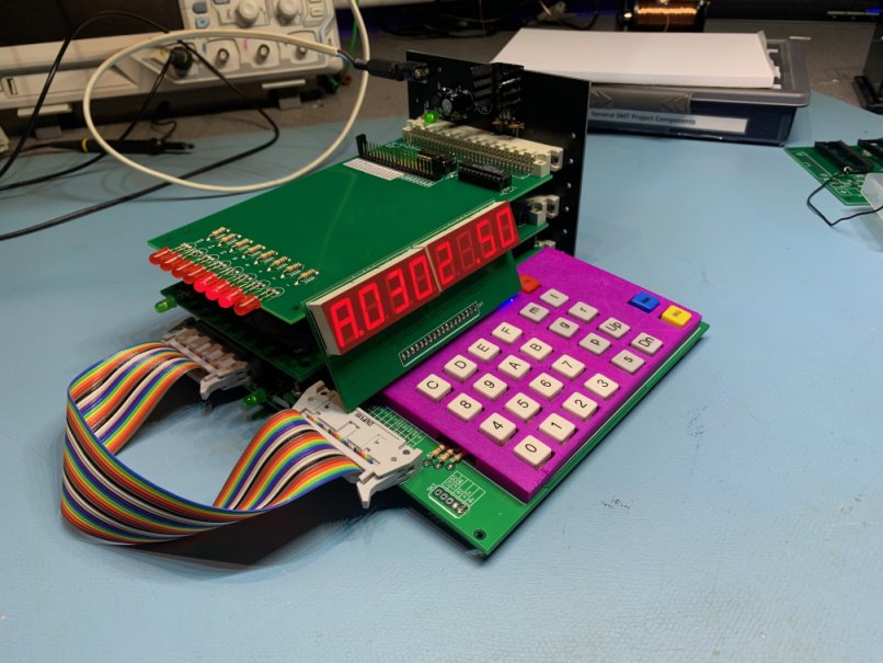
Above you can see a SAD board and it inserted into the 3 slot backplane along with the System 1 CPU card and an 8-bit LED display card.
It’s typical that each expansion card will need one address or block of addresses; it’s not very common that a single card needs multiple ranges of addresses but this is possible if required.
Using the SAD you can supply an expansion card with either one or more 4K block(s), one or more 256 byte page(s) and one or more 16 bit segment(s). The 8-bit LED card shown above has a simple 8 to 1 decoder on-board so it can decode the lower or upper 8 bytes of the 16 byte segment address; and it’s accomplished with just one cheap 74LS138 IC. This means that you could install 16 of the 8-bit LED cards and they would all only need one MAP signal representing a single segment between them. It’s very efficient in address space and components.
Construction details, schematics and plans can be found here.
Leave a Reply
You must be logged in to post a comment.