
What can I say… I’m a busy chap.
I’ve been so busy with work and a large personal project that I’ve not really had much time for “fun” things, that said, it’s funny how one thing leads to another.
I’ve been working on an all consuming huge project and I needed to take a break. I’m at a bit where I’m stuck and so decided to distract myself for a while and do something fun.
Many many years ago I had a project; the Digital IC Tester, published by Everyday Practical Electronics a UK electronics magazine. It consisted of a PCB with a PIC micro, some jellybean components and a serial connection to a PC that ran some; though I say so myself, brilliantly designed and written software. The setup was capable of testing TTL and CMOS digital ICs and the user could add their own IC definitions to the database. It wasn’t meant to test all the operational parameters of an IC, just give a go/no go indication of it’s operation. The project was a huge success apparently and even now I get e-mails about it. The software has been ported from Windows to other platforms and people have reinvented the design to suit their own requirements… it’s been rather good 🙂
The reason I’m bleating on about this piece of history is that over the years I’ve had to fend off one question repeatedly “will it test ICs in-circuit”.
The simple answer is “no”.. it won’t. The more complex answer is still “no”.
If you imagine an IC as part of a larger circuit, the IC inputs are connected to other components in the circuit that are attempting to drive those inputs. You cannot just attach a test clip and start trying to force pins to logic levels when those pins are attached to other components in the circuit that are themselves trying to drive the same pins.
Attempting this would probably either damage these components in the circuit, or the tester device.
However, some while ago I had a thought.
Imagine a circuit; as complex as you like, that contains a suspect IC; and for sake of explanation and simplicity we will pick the humble 74LS00 – Quad 2-input NAND.
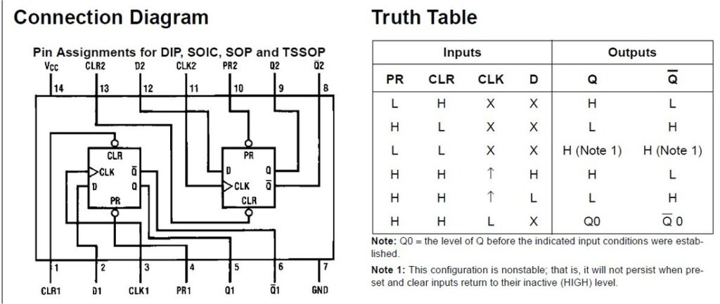
The IC contains four NAND gates, where each gate contains two input pins and one output pin. With two inputs there are four possible logic output combinations. Details of the logic combinations and related output logic levels are listed in the truth table or function table for the gate.
The common way to test the IC is to manipulate the logic levels on the input pins, monitor the output logic level and compare the results with the published truth table. If the output logic levels deviate from the truth table, it’s fair to assume the IC is faulty.
It occurred to me that I don’t have to drive the inputs, the circuit will do that. All I need to do is capture the logic levels on the inputs and outputs and compare them with the truth table.
There is a flaw in this plan… actually it turns out there are two flaws but I didn’t see the second until after I tried… But more on that exciting revelation in a minute.
As already stated, out NAND gate has two inputs which gives a total of four possible input logic level combinations. But what if the circuit never uses all four combinations ?
If I capture the input and output logic levels and compare them with the truth table, I can state that I know how many input combinations are possible (four for our NAND gate), that I’ve only detected some of them, (for example lets assume only three of the combinations have been used), and of those three combinations detected they all gave the correct logical output. So I’m 75% confidant the NAND gate is working correctly. If however I detect an invalid logic output for an input combination, I can be 100% confidant that the NAND gate is faulty.
It’s brilliant.
Actually… it’s almost brilliant.
I rushed to my breadboard and constructed a simple test circuit.
I would use a parallel load shift register to take a snapshot of the logic levels on all the IC pins, and then compare that data to the truth table from the data sheet.
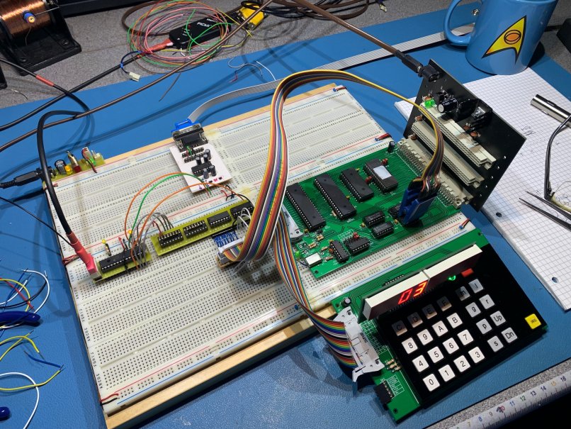
The above picture shows my prototype.
A 16-bit shift register with parallel load inputs is connected via a ribbon cable to an IC under test; the IC was in fact a 74LS00 running on my perfectly working 6502 CPU card.
The data is read from the shift register by a PIC micro and the data squirted down a serial connection to my PC that was running a bit of VB code to display the results. This was going to be great.
It worked, data was being captured in real-time and I could see the logic combinations being displayed on screen.
Then I noticed something strange..
I was getting more combinations detected than were possible for a NAND gate.
I would see both inputs at logic 0 but the output also logic 0, or both inputs at logic 1, and the output also at logic 1. This wasn’t possible unless there was a fault somewhere, and I knew that the IC was fine as was the CPU card being tested.
Time to break out the logic analyser.
Ok, on reflection I should have done this first, it would have saved a lot of trouble later on. But it was on the top shelf under a pile of junk and a P.I.T.A to get too.
After a couple of minutes the problem became obvious.

The three traces represent pins 1, 2 & 3 (1,2 are inputs and 3 is the output) of a 2-input NAND gate.
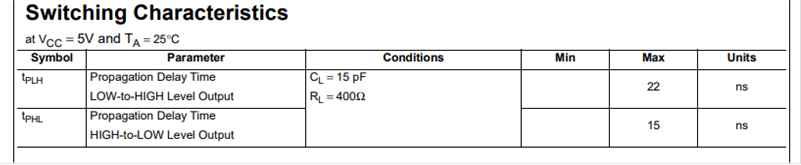
The trace shows that pin 2 (middle trace) is at logic 1 constantly, and then shows pin 1 moving from logic 0 to logic 1. However, you can see there is a delay before the gate output (lower trace) moves from logic 1 to logic 0.
This delay is the gate propagation delay, and if, unlike me, you take the time to actually read the datasheet for the humble 74LS00 in detail, you will see it states the propagation delay as a maximum of 15ns (it’s around 10ns on the logic trace so that’s within specification).
So, what next.. is the great invention dead.
Well I think that using my hardware project to capture the data is not going to work. Whilst I originally didn’t need to capture every logic change it’s really not going to be fast enough.
I did try a different hardware setup that used 74LS573 8-bit latches to capture the data but it still takes too long to read the data, store it in the PIC and then transmit back to the PC. Even buffering a batch of results in the PIC first wasn’t fast enough.
Then I thought, but my logic analyser “is” fast enough… and it has a very nice data export function. I could capture the data and export it for processing by my own software.
If I watch for logic changes on the pins designated as outputs, and then backtrack in time I should be able to find the value of the input pins. It might work.
Next problem which I never thought was going to be a problem… I need a 20 and/or 16 pin IC test clip.
I’ve a 14 and a 40 pin one that I’ve had for years, so I went shopping for a 16 and 20 pin versions. Have you seen the price of IC test clips in the UK?… they are absolutely ridiculous.
After seeing the price I started wondering if I could make my own.
Question, can my 3D printer, print the case for a test-clip that is high detail but strong enough to make a decent test clip?
So I designed this in TinkerCad…
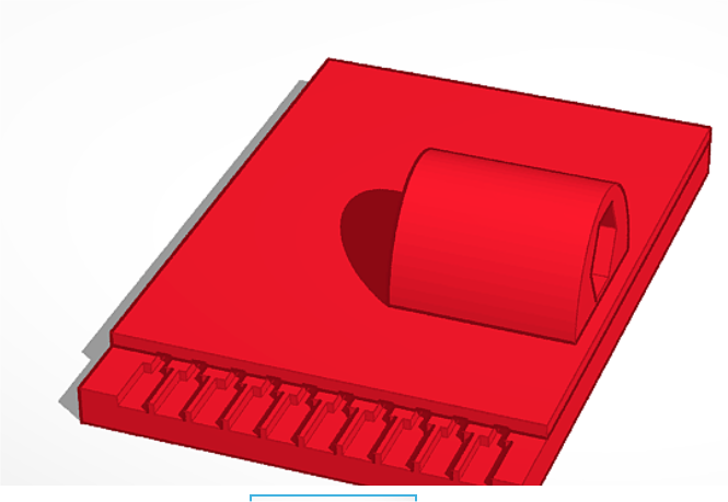
And yes… it can give the resolution required and seems strong enough.
The above model has ten hollow channels that run from the pin contact area all the way to the top and will allow for a fine connecting wire. I just need to figure out what I can use to make the contact.
After this, print two identical copies, fit a torsion spring and a bolt and it should be done.
If anybody out there reading this is into hobby electronics I cannot recommend strongly enough that you have a look at 3D printing if you’ve not already. They are quite affordable these days and as long as you aren’t overly bothered about keeping lots of different colours of filament in stock (I only print on whatever colour I last purchased as cheaply as I could find it), it’s not very expensive to use.
Considering that one supplier wanted over £100 for a 20 pin test clip… printing your own small parts and tools can be a real cost saving.
Leave a Reply
You must be logged in to post a comment.