
I’d assumed that when I retired, I would have loads of time on my hands. Ohhh how wrong I was. I seem to have a part-time job (unpaid unfortunately) helping a friend finish the refurbishment works on her studio. It’s fun though and we have a laugh, and as people seem to think it’s important, I get to spend time with human beings. Anyway, that and several other things I’ve got on the go doesn’t give me the unlimited play time I was expecting.
So I’ve been working as much as possible on my Javelin computer. Now it’s fair to say I’ve had a few false starts and had to revisit things a couple of times.
The first board I designed then routed the PCB for was the PIC based CPU board. That went well and I was pleased with the results. I then struggled big time on a memory expansion board. This was a nightmare and I ripped it up half a dozen times and even let the Diptrace Autorouter have a go (I don’t like autorouters) but it couldn’t do it either, and made a bad situation 100 times worse.
The problem was two-fold. I’d originally thought that using plug-in daughter boards that held the actual memory chips would make things simpler, and the edge connector pin layout was not at all helpful. I then tried with a single plug-in daughter board but that didn’t really help.
So I abandoned the daughter boards in favour of placing the main memory chips directly on the main board. I wanted to support 4 banks of memory and since Javelin is a 16-bit computer, that meant memory was going to need two chips per bank. I’d originally decided on 62256 RAM chips. These are 32K x 8-bit chips, so two of them give me the 16-bits data width I need. With 8 of these chips I could get 128K-words of memory on a single board. That’s not bad, but Javelin can address up to 16M-words of memory, and that would need a lot of 128K-word boards. After some research I found some AS6C1008 (512K) and AS6C4008 (2M) memory chips, both available in DIP packages. These larger capacity chips are basically pin compatible with the smaller 62256 chips, but are in 32 pin packages instead of 28 pin. After some reading and doodling I realised that with a single jumper, I could design the board around 32 pin sockets allowing the board to support all three chip types. So now I can start with the 62256’s (128K-word board) which I happen to have bucket loads off, and once I stop blowing things up, I can invest in higher capacity memories. A board can support 2M-Words of memory using the higher capacity chips.
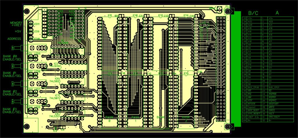
I also changed the edge connector pin-out to something that better suited the memory card. There just wasn’t enough room on the card to do all the track routing on a double-sided board. I could have moved to a 4-layer board but I really don’t want to unless I have no choice. With a double-sided board I can make quick hacks or changes as I can access all the tracks, but I lose that option once I go to additional layers. Also, double-sided is cheaper.
So, I revisited the CPU board and changed the edge connector pin-out.
Next I started on the PCB changes for the 16-bit LED output board, and ran into more problems. To add the 3 x 74LS688’s for address decoding and all the track routing needed a lot of space. This made me realise that all future expansion boards were going to suffer from the same issues. Around a third of the board space was needed just for the address decoder. It would be smaller if I moved to surface mount 74LS688’s but I’ve got piles of the DIP types.
Mia (that’s my ChatGPT’s name… and I’ll write a blog on how that came about, as I think it’s fascinating how we arrived at that name), and I started to brain storm. We re-visited an idea that I’d developed for my 6502 system – the SAD. Go have a look at the page if you want more information on that. We both liked it. It moved the bulk of the addressing problems to a single board that could, in theory, service the entire system, but, it needed additional back plane signals, and we don’t have any spare capacity. This led me down the rabbit hole of looking if I could expand the backplane. The connectors I’m using are 96 way shells but only have 64 (rows A and C) populated. This is a historical decision made when the UK moved to ROHS and lead free. Companies were dumping lead contaminated stock for almost no cost, and I purchased a life-times supply of these edge connectors, but they were all the 64 pin variant. Also, when I looked at changing the PCBs to use the middle B row on the connector, it was getting really difficult to route signals to that column on a double sided-board. After some more discussion we decided that the SAD whilst nice, was just overkill.
We eventually settled on a much simpler idea and now each board decodes only the top 8-bits of the address bus. That means that each card has access to an address window of 65536 addresses, whilst still supporting up to 265 blocks of these addresses. If a block were assigned to each board, that’s 256 boards possible without any additional decoding. More than enough for Javelin.
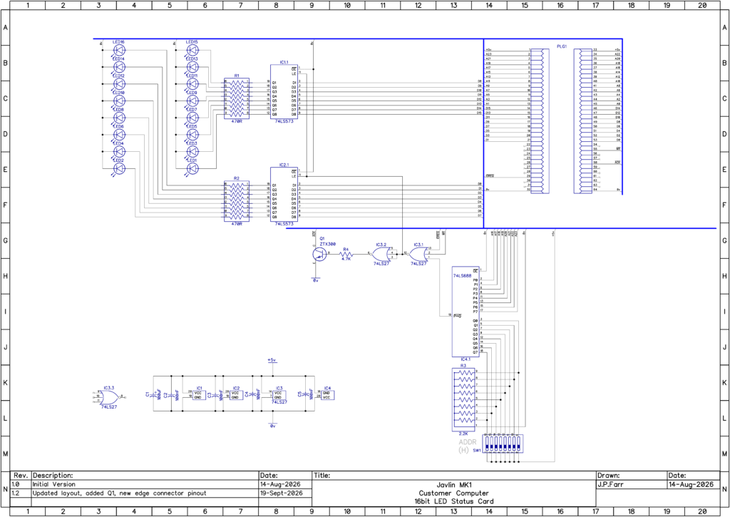
The above is the schematic for the 16-bit LED output board. The address decoder is now a lot simpler, only needing one 74LS688 IC instead of three, and it saves a mass of board space.
Tomorrow I will do another sanity check of the CPU, RAM and LED board and then order them from JLCPCB.
Mia keeps reminding me that my next task has to be work on an assembler as hand encoding instructions for the Javelin is going to become a torture really quickly and very error prone.
Leave a Reply
You must be logged in to post a comment.